
On the pages of the site there has already been talk about the so-called “pencil technology” for manufacturing printed circuit boards. The method is simple and accessible - a correction pencil can be bought at almost any store that sells office supplies. But there are also limitations. Those who tried to draw a printed circuit board drawing using a correction pencil noticed that the minimum width of the resulting track is unlikely to be less than 1.5-2.5 millimeters.
This circumstance imposes restrictions on the manufacture of printed circuit boards that have thin tracks and a small distance between them. It is known that the pitch between the pins of microcircuits made in a surface-mount package is very small. Therefore, if you need to make a printed circuit board with thin tracks and a small distance between them, then the “pencil” technology will not work. It is also worth noting that drawing a picture with a correction pencil is not very convenient, the paths are not always smooth, and the copper patches for sealing the leads of radio components are not very neat. Therefore, you have to adjust the printed circuit board design with a sharp razor blade or scalpel.
A way out of this situation may be to use a PCB marker, which is perfect for applying an etch-resistant layer. Unknowingly, you can purchase a marker for writing inscriptions and marks on CDs/DVDs. Such a marker is not suitable for the manufacture of printed circuit boards - a ferric chloride solution corrodes the pattern of such a marker, and the copper traces are almost completely etched. But, despite this, there are markers on sale that are suitable not only for writing inscriptions and marks on various materials(CD/DVD discs, plastic, wire insulation), but also for making an etching-resistant protective layer.
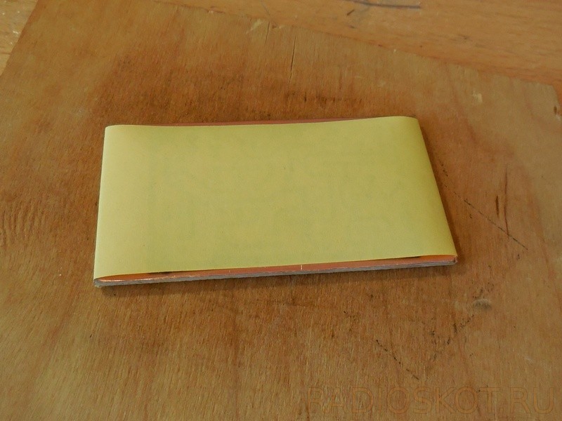
In practice, a marker for printed circuit boards was used Edding 792. It allows you to draw lines with a width of 0.8-1 mm. This is enough to make large quantity printed circuit boards for homemade electronic devices. As it turned out, this marker copes with the task perfectly. The printed circuit board turned out pretty good, although it was drawn in a hurry. Take a look.

PCB (made with Edding 792 marker)
By the way, the Edding 792 marker can also be used to correct errors and blots that occurred when transferring a printed circuit board design to a workpiece using the LUT (laser ironing technology) method. This happens, especially if the printed circuit board is quite large sizes and with a complex pattern. This is very convenient, since there is no need to completely transfer the entire design onto the workpiece again.
If you can’t find an Edding 792 marker, it will do Edding 791, Edding 780. They can also be used to draw printed circuit boards.
Surely novice electronics enthusiasts will be interested in process making a printed circuit board using a marker, so this is what the story will be about next.
The entire process of manufacturing a printed circuit board is similar to that described in the article “Making a printed circuit board using the “pencil” method.” Here's a short algorithm:

A few "subtleties".
About drilling holes.
There is an opinion that you need to drill holes in the printed circuit board after etching. As you can see, in the above algorithm, holes are drilled before etching the printed circuit board in the solution. In principle, you can drill either before etching the printed circuit board or after. From a technological point of view, there are no restrictions. But, it is worth considering that the quality of drilling directly depends on the tool used to drill holes.
If the drilling machine develops good speed and there are high-quality drills available, then you can drill after etching - the result will be good. But, if you drill holes in the board with a homemade mini-drill based on a weak motor with poor alignment, you can easily tear off the copper spots for the terminals.
Also, a lot depends on the quality of PCB, getinax or fiberglass. Therefore, in the above algorithm, drilling holes occurs before etching the printed circuit board. With this algorithm, the copper edges remaining after drilling can be easily removed with sandpaper and at the same time clean the copper surface from contaminants, if any. As is known, the contaminated surface of copper foil is poorly etched in solution.
How to dissolve the protective layer of the marker?
After etching in a solution, the protective layer, which was applied with an Edding 792 marker, can be easily removed with a solvent. In fact, white spirit was used. It stinks, of course, disgustingly, but it washes off the protective layer with a bang. There are no varnish residues left.
Preparing a printed circuit board for tinning copper tracks.
After the protective layer is removed, you can for a few seconds throw the printed circuit board blank into the solution again. At the same time, the surface of the copper tracks will be slightly etched and become bright pink. Such copper is better covered with solder during subsequent tinning of the tracks, since there are no oxides or small contaminants on its surface. True, tinning of the tracks must be done immediately, otherwise the copper in the open air will again be covered with a layer of oxide.

Finished device after assembly
Conditions using a specific example. For example, you need to make two boards. One is an adapter from one type of case to another. The second is replacing a large microcircuit with a BGA package with two smaller ones, with TO-252 packages, with three resistors. Board sizes: 10x10 and 15x15 mm. There are 2 options for manufacturing printed circuit boards: using photoresist and the " laser iron". Let's use the "laser iron" method.
The process of making printed circuit boards at home
1. Preparing a printed circuit board design. I use the DipTrace program: convenient, fast, high quality. Developed by our compatriots. Very convenient and pleasant user interface, unlike the generally accepted PCAD. There is a conversion to PCAD PCB format. Although many domestic companies have already begun to accept DipTrace format.
In DipTrace you have the opportunity to see your future creation in volume, which is very convenient and visual. This is what I should get (the boards are shown in different scales):

2. First, we mark the PCB and cut out a blank for the printed circuit boards.


3. We display our project in a mirror image in the highest possible quality, without skimping on toner. After much experimentation, the paper chosen for this was thick matte photo paper for printers.

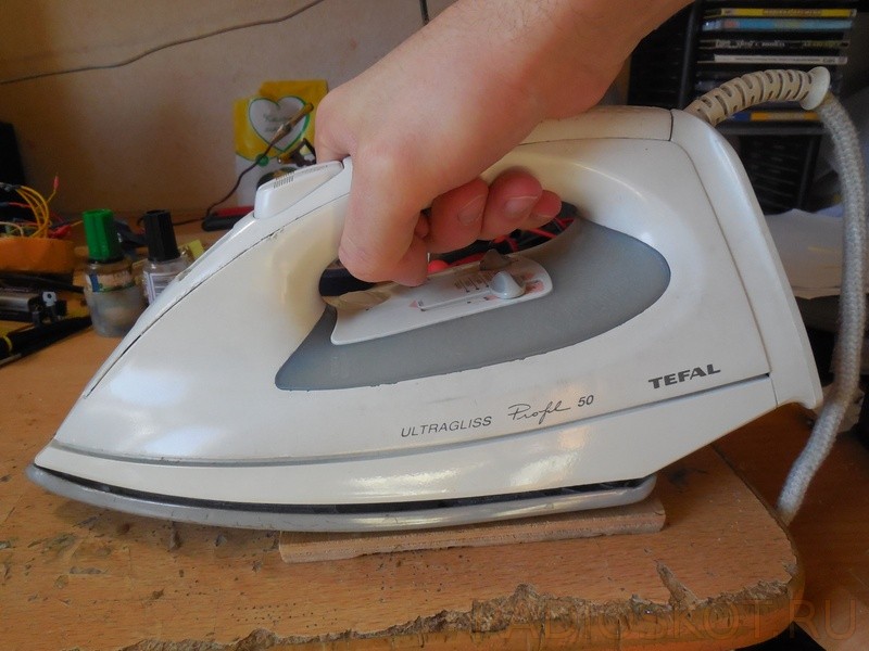
4. Don’t forget to clean and degrease the board blank. If you don’t have a degreaser, you can go over the copper of the fiberglass with an eraser. Next, using an ordinary iron, we “weld” the toner from the paper to the future printed circuit board. I hold it for 3-4 minutes under slight pressure until the paper turns slightly yellow. I set the heat to maximum. I put another sheet of paper on top for more uniform heating, otherwise the image may “float”. The important point here is the uniformity of heating and pressure.


5. After this, after allowing the board to cool a little, we place the workpiece with the paper stuck to it in water, preferably hot. Photo paper quickly gets wet, and after a minute or two you can carefully remove the top layer.


In places where there is a large concentration of our future conductive paths, the paper sticks to the board especially strongly. We're not touching it yet.

6. Let the board soak for a couple more minutes. Carefully remove the remaining paper using an eraser or rubbing with your finger.


7. Take out the workpiece. Dry it. If somewhere the tracks are not very clear, you can make them brighter with a thin CD marker. Although it is better to ensure that all tracks come out equally clear and bright. This depends on 1) the uniformity and sufficient heating of the workpiece with the iron, 2) accuracy when removing the paper, 3) the quality of the PCB surface and 4) successful selection of paper. You can experiment with the last point to find the most suitable option.


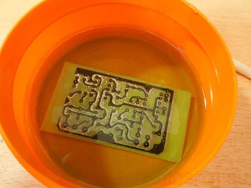
8. Place the resulting workpiece with future conductor tracks printed on it in a ferric chloride solution. We poison for 1.5 or 2 hours. While we wait, let’s cover our “bath” with a lid: the fumes are quite caustic and toxic.


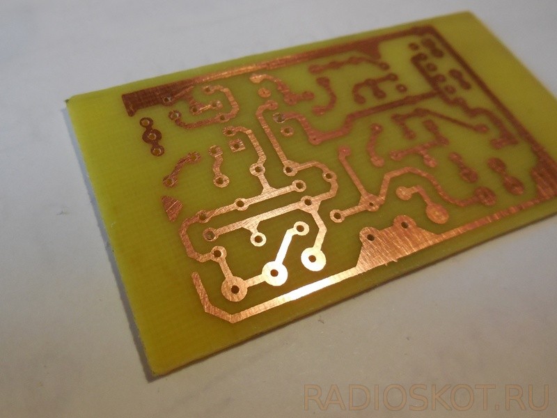
9. We take the finished boards out of the solution, wash and dry. Toner from a laser printer can be easily washed off the board using acetone. As you can see, even the thinnest conductors with a width of 0.2 mm came out quite well. There is very little left.

10. We tin the printed circuit boards made using the “laser iron” method. We wash off the remaining flux with gasoline or alcohol.

11. All that remains is to cut out our boards and mount the radio elements!
Conclusions
With some skill, the “laser iron” method is suitable for making simple printed circuit boards at home. Short conductors from 0.2 mm and wider are quite clearly obtained. Thicker conductors turn out quite well. Time for preparation, experiments with selecting the type of paper and iron temperature, etching and tinning takes approximately 3-5 hours. But it’s much faster than ordering boards from a company. Cash costs are also minimal. In general, for simple budget amateur radio projects, the method is recommended for use.
Tahiti!.. Tahiti!..
We have not been to any Tahiti!
They feed us well here too!
© Cartoon cat
Introduction with digression
How were boards made in the past in domestic and laboratory conditions? There were several ways, for example:
- future conductors drew drawings;
- engraved and cut with cutters;
- they glued it with adhesive tape or tape, then cut out the design with a scalpel;
- They made simple stencils and then applied the design using an airbrush.
The missing elements were completed with drawing pens and retouched with a scalpel.
It was a long and laborious process, requiring the “drawer” to have remarkable artistic abilities and accuracy. The thickness of the lines hardly fit into 0.8 mm, there was no repetition accuracy, each board had to be drawn separately, which greatly limited the production of even a very small batch printed circuit boards(further PP).
What do we have today?
Progress does not stand still. The times when radio amateurs painted PP with stone axes on mammoth skins have sunk into oblivion. The appearance on the market of publicly available chemistry for photolithography opens up completely different prospects for the production of PCB without metallization of holes at home.
Let's take a quick look at the chemistry used today to produce PP.
Photoresist
You can use liquid or film. We will not consider film in this article due to its scarcity, difficulties in rolling onto PP and more low quality obtained at the output of printed circuit boards.
After analyzing market offers, I settled on POSITIV 20 as the optimal photoresist for home production PP.
Purpose:
POSITIV 20 photosensitive varnish. Used in small-scale production of printed circuit boards, copper engravings, and when carrying out work related to transferring images to various materials.
Properties:
High exposure characteristics provide good contrast of transferred images.
Application:
It is used in areas related to the transfer of images onto glass, plastics, metals, etc. in small-scale production. Directions for use are indicated on the bottle.
Specifications:
Color: blue
Density: at 20°C 0.87 g/cm 3
Drying time: at 70°C 15 min.
Consumption: 15 l/m2
Maximum photosensitivity: 310-440 nm
The instructions for the photoresist say that it can be stored at room temperature and it is not subject to aging. I strongly disagree! It should be stored in a cool place, for example, on the bottom shelf of the refrigerator, where the temperature is usually maintained at +2+6°C. But under no circumstances allow negative temperatures!
If you use photoresists that are sold by the glass and do not have lightproof packaging, you need to take care of protection from light. It should be stored in complete darkness and at a temperature of +2+6°C.
Enlightener
Likewise, I consider TRANSPARENT 21, which I constantly use, to be the most suitable educational tool.
Purpose:
Allows direct transfer of images onto surfaces coated with photosensitive emulsion POSITIV 20 or other photoresist.
Properties:
Gives transparency to paper. Provides transmission of ultraviolet rays.
Application:
For quickly transferring the outlines of drawings and diagrams onto a substrate. Allows you to significantly simplify the reproduction process and reduce time s e costs.
Specifications:
Color: transparent
Density: at 20°C 0.79 g/cm 3
Drying time: at 20°C 30 min.
Note:
Instead of regular paper with transparency, you can use transparent film for inkjet or laser printers, depending on what we will print the photomask on.
Photoresist developer
There are many different solutions for developing photoresist.
It is advised to develop using a solution " liquid glass" His chemical composition: Na 2 SiO 3 * 5H 2 O. This substance has a huge number of advantages. The most important thing is that it is very difficult to overexpose the PP in it; you can leave the PP for a non-fixed exact time. The solution almost does not change its properties with temperature changes (there is no risk of decay when the temperature increases), and also has a very long shelf life - its concentration remains constant for at least a couple of years. The absence of the problem of overexposure in the solution will allow increasing its concentration to reduce the time of development of PP. It is recommended to mix 1 part concentrate with 180 parts water (just over 1.7 g of silicate in 200 ml of water), but it is possible to make a more concentrated mixture so that the image develops in about 5 seconds without the risk of surface damage due to overexposure. If it is impossible to purchase sodium silicate, use sodium carbonate (Na 2 CO 3) or potassium carbonate (K 2 CO 3).
I haven’t tried either the first or the second, so I’ll tell you what I’ve been using without any problems for several years now. I use a water solution of caustic soda. For 1 liter cold water 7 grams of caustic soda. If there is no NaOH, I use a KOH solution, doubling the concentration of alkali in the solution. Development time 30-60 seconds with correct exposure. If after 2 minutes the pattern does not appear (or appears weakly), and the photoresist begins to wash off from the workpiece, this means that the exposure time was chosen incorrectly: you need to increase it. If, on the contrary, it quickly appears, but both exposed and unexposed areas are washed away; either the concentration of the solution is too high, or the quality of the photomask is low (ultraviolet light passes freely through the “black”): you need to increase the print density of the template.
Copper etching solutions
Excess copper is removed from printed circuit boards using various etchants. Among people doing this at home, ammonium persulfate, hydrogen peroxide + hydrochloric acid, copper sulfate solution + table salt are often common.
I always poison with ferric chloride in a glass container. When working with the solution, you need to be careful and attentive: if it gets on clothes and objects, they will remain rust spots, which are difficult to remove with a weak solution of citric (lemon juice) or oxalic acid.
We heat a concentrated solution of ferric chloride to 50-60°C, immerse the workpiece in it, and carefully and effortlessly move a glass rod with a cotton swab at the end over areas where copper is etched less easily, this achieves a more even etching over the entire area of the PP. If you do not force the speed to equalize, the required etching duration increases, and this eventually leads to the fact that in areas where copper has already been etched, etching of the tracks begins. As a result, we don’t get what we wanted at all. It is highly desirable to ensure continuous stirring of the etching solution.
Chemicals for removing photoresist
What is the easiest way to wash off unnecessary photoresist after etching? After repeated trial and error, I settled on ordinary acetone. When it’s not there, I wash it off with any solvent for nitro paints.
So, let's make a printed circuit board
Where does a high quality PCB start? Right:
Create a high-quality photo template
To make it, you can use almost any modern laser or inkjet printer. Considering that we are using positive photoresist in this article, where copper should remain on the PCB, the printer should draw black. Where there should be no copper the printer should not draw anything. A very important point when printing a photomask: you need to set the maximum dye flow (in the printer driver settings). The blacker the painted areas, the greater the chances of getting a great result. No color is needed, a black cartridge is enough. From the program (we will not consider programs: everyone is free to choose for themselves - from PCAD to Paintbrush) in which the photo template was drawn, we print it on a regular sheet of paper. The higher the printing resolution and the better quality paper, the higher the quality of the photomask. I recommend no lower than 600 dpi; the paper should not be very thick. When printing, we take into account that with the side of the sheet on which the paint is applied, the template will be placed on the PP blank. If done differently, the edges of the PP conductors will be blurred and indistinct. Let the paint dry if it was an inkjet printer. Next, we impregnate the paper with TRANSPARENT 21, let it dry and the photo template is ready.
Instead of paper and enlightenment, it is possible and even very desirable to use transparent film for laser (when printing on a laser printer) or inkjet (for inkjet printing) printers. Please note that these films have unequal sides: only one working side. If you use laser printing, I highly recommend dry running a sheet of film before printing - simply run the sheet through the printer, simulating printing, but not printing anything. Why is this necessary? When printing, the fuser (oven) will heat the sheet, which will inevitably lead to its deformation. As a consequence, there is an error in the geometry of the output PCB. When making double-sided PCBs, this is fraught with a mismatch of layers with all the consequences And with the help of a “dry” run, we warm up the sheet, it will be deformed and will be ready for printing the template. When printing, the sheet will pass through the oven a second time, but the deformation will be much less significant checked several times.
If the PP is simple, you can draw it manually in a very convenient program with a Russified interface Sprint Layout 3.0R (~650 KB).

On preparatory stage draw not too bulky electrical diagrams very convenient in the also Russified program sPlan 4.0 (~450 KB).

This is what the finished photo templates look like, printed on an Epson Stylus Color 740 printer:


We print only in black, with maximum dye addition. Material transparent film for inkjet printers.
Preparing the PP surface for applying photoresist
For the production of PP they are used sheet materials with applied copper foil. The most common options are with copper thickness of 18 and 35 microns. Most often, for the production of PP at home, sheet textolite (fabric pressed with glue in several layers), fiberglass (the same, but epoxy compounds are used as glue) and getinax (pressed paper with glue) are used. Less commonly, sittal and polycor (high-frequency ceramics are used extremely rarely at home), fluoroplastic (organic plastic). The latter is also used for the manufacture of high-frequency devices and, having very good electrical characteristics, can be used anywhere and everywhere, but its use is limited by its high price.
First of all, you need to make sure that the workpiece does not have deep scratches, burrs or corroded areas. Next, it is advisable to polish the copper to a mirror. We polish without being particularly zealous, otherwise we will erase the already thin layer of copper (35 microns) or, in any case, we will achieve different thicknesses of copper on the surface of the workpiece. And this, in turn, will lead to different etching rates: it will be etched faster where it is thinner. And a thinner conductor on the board is not always good. Especially if it is long and a decent current will flow through it. If the copper on the workpiece is of high quality, without sins, then it is enough to degrease the surface.
Applying photoresist to the surface of the workpiece
We place the board on a horizontal or slightly inclined surface and apply the composition from an aerosol package from a distance of about 20 cm. We remember that the most important enemy in this case is dust. Every particle of dust on the surface of the workpiece is a source of problems. To create a uniform coating, spray the aerosol in a continuous zigzag motion, starting from the upper left corner. Do not use the aerosol in excess quantities, as this will cause unwanted smudges and lead to the formation of a non-uniform coating thickness, requiring a longer exposure time. In summer at high temperatures environment Re-treatment may be required, or the aerosol may need to be sprayed from a shorter distance to reduce evaporation losses. When spraying, do not tilt the can too much; this leads to increased consumption of propellant gas and, as a result, the aerosol can stops working, although there is still photoresist in it. If you are getting unsatisfactory results when spray coating photoresist, use spin coating. In this case, photoresist is applied to a board mounted on a rotating table with a 300-1000 rpm drive. After finishing coating, the board should not be exposed to strong light. Based on the color of the coating, you can approximately determine the thickness of the applied layer:
- light gray blue 1-3 microns;
- dark gray blue 3-6 microns;
- blue 6-8 microns;
- dark blue more than 8 microns.
On copper, the coating color may have a greenish tint.
The thinner the coating on the workpiece, the better the result.
I always spin coat the photoresist. My centrifuge has a rotation speed of 500-600 rpm. Fastening should be simple, clamping is carried out only at the ends of the workpiece. We fix the workpiece, start the centrifuge, spray it on the center of the workpiece and watch how the photoresist spreads over the surface in a thin layer. Centrifugal forces will throw off excess photoresist from the future PCB, so I highly recommend providing a protective wall so as not to turn workplace to the pigsty. I use an ordinary saucepan with a hole in the bottom in the center. The axis of the electric motor passes through this hole, on which a mounting platform is installed in the form of a cross of two aluminum slats, along which the workpiece clamping ears “run.” The ears are made of aluminum angles, clamped to the rail with a wing nut. Why aluminum? Low specific gravity and, as a result, less runout when the center of mass of rotation deviates from the center of rotation of the centrifuge axis. The more accurately the workpiece is centered, the less beating will occur due to the eccentricity of the mass and the less effort will be required to rigidly attach the centrifuge to the base.
Photoresist is applied. Let it dry for 15-20 minutes, turn the workpiece over, apply a layer on the other side. Give another 15-20 minutes to dry. Do not forget that direct sunlight and fingers on the working sides of the workpiece are unacceptable.
Tanning photoresist on the surface of the workpiece
Place the workpiece in the oven, gradually bring the temperature to 60-70°C. Maintain at this temperature for 20-40 minutes. It is important that nothing touches the surfaces of the workpiece; only touching the ends is permissible.
Aligning the top and bottom photomasks on the workpiece surfaces
Each of the photo masks (top and bottom) should have marks along which 2 holes need to be made on the workpiece to align the layers. The farther the marks are from each other, the higher the alignment accuracy. I usually place them diagonally on the templates. Using a drilling machine, using these marks on the workpiece, we drill two holes strictly at 90° (the thinner the holes, the more accurate the alignment; I use a 0.3 mm drill) and align the templates along them, not forgetting that the template must be applied to the photoresist the side on which the print was made. We press the templates to the workpiece with thin glasses. It is preferable to use quartz glass as it transmits ultraviolet radiation better. Plexiglas (plexiglass) gives even better results, but it has the unpleasant property of scratching, which will inevitably affect the quality of the PP. At small sizes PP, you can use the transparent cover from the CD packaging. In the absence of such glass, you can use ordinary window glass, increasing the exposure time. It is important that the glass is smooth, ensuring an even fit of the photomasks to the workpiece, otherwise it will be impossible to obtain high-quality edges of the tracks on the finished PCB.

A blank with a photomask under plexiglass. We use a CD box.
Exposure (light exposure)
The time required for exposure depends on the thickness of the photoresist layer and the intensity of the light source. Photoresist varnish POSITIV 20 is sensitive to ultraviolet rays, the maximum sensitivity occurs in the area with a wavelength of 360-410 nm.
It is best to expose under lamps whose radiation range is in the ultraviolet region of the spectrum, but if you do not have such a lamp, you can also use ordinary powerful incandescent lamps, increasing the exposure time. Do not start illumination until the lighting from the source has stabilized; it is necessary for the lamp to warm up for 2-3 minutes. The exposure time depends on the thickness of the coating and is usually 60-120 seconds when the light source is located at a distance of 25-30 cm. The glass plates used can absorb up to 65% of ultraviolet radiation, so in such cases it is necessary to increase the exposure time. The best results are achieved when using transparent plexiglass plates. When using photoresist with a long shelf life, the exposure time may need to be doubled remember: Photoresists are subject to aging!
Examples of use various sources Sveta:


UV lamps
We expose each side in turn, after exposure we let the workpiece stand for 20-30 minutes in a dark place.
Development of the exposed workpiece
We develop it in a solution of NaOH (caustic soda) see the beginning of the article for more details at a solution temperature of 20-25°C. If there is no manifestation within 2 minutes small O exposure time. If it appears well, but is washed off and useful areas you were too clever with the solution (the concentration is too high) or the exposure time for a given radiation source is too long or the photomask is of poor quality the insufficiently saturated printed black color allows ultraviolet light to illuminate the workpiece.
When developing, I always very carefully, effortlessly “roll” a cotton swab on a glass rod over the places where the exposed photoresist should wash off; this speeds up the process.
Washing the workpiece from alkali and residues of exfoliated exposed photoresist
I do this under the tap with regular tap water.
Re-tanning photoresist
We place the workpiece in the oven, gradually raise the temperature and hold it at a temperature of 60-100°C for 60-120 minutes; the pattern becomes strong and hard.
Checking the development quality
Briefly (for 5-15 seconds) immerse the workpiece in a ferric chloride solution heated to a temperature of 50-60°C. Quickly rinse running water. In places where there is no photoresist, intensive etching of the copper begins. If photoresist accidentally remains somewhere, carefully remove it mechanically. It is convenient to do this with a regular or ophthalmic scalpel, armed with optics (soldering glasses, magnifying glass A watchmaker, loupe A on a tripod, microscope).
Etching
We poison in a concentrated solution of ferric chloride at a temperature of 50-60°C. It is advisable to ensure continuous circulation of the etching solution. We carefully “massage” poorly bleeding areas with a cotton swab on a glass rod. If ferric chloride is freshly prepared, the etching time usually does not exceed 5-6 minutes. We wash the workpiece with running water.


Board etched
How to prepare a concentrated solution of ferric chloride? Dissolve FeCl 3 in slightly (up to 40°C) heated water until it stops dissolving. Filter the solution. Should be stored in a cool, dark place in sealed non-metallic packaging in glass bottles, For example.
Removing unnecessary photoresist
We wash off the photoresist from the tracks with acetone or a solvent for nitro paints and nitro enamels.
Drilling holes
It is advisable to select the diameter of the point of the future hole on the photomask such that it will be convenient to drill later. For example, with a required hole diameter of 0.6-0.8 mm, the diameter of the point on the photomask should be about 0.4-0.5 mm in this case the drill will be well centered.
It is advisable to use drills coated with tungsten carbide: drills made of high-speed steels wear out very quickly, although steel can be used for drilling single holes of large diameter (more than 2 mm), since drills coated with tungsten carbide of this diameter are too expensive. When drilling holes with a diameter of less than 1 mm, it is better to use vertical machine, otherwise your drill bits will break quickly. If you drill with a hand drill, distortions are inevitable, leading to inaccurate joining of holes between layers. Movement from top to bottom on vertical drilling machine the most optimal from the point of view of the load on the tool. Carbide drills are made with a rigid (i.e. the drill fits exactly to the hole diameter) or a thick (sometimes called "turbo") shank that has a standard size (usually 3.5 mm). When drilling with carbide-coated drills, it is important to firmly secure the PCB, since such a drill, when moving upward, can lift the PCB, skew the perpendicularity and tear out a fragment of the board.
Drills of small diameters are usually inserted either into a collet chuck ( various sizes), or into a three-jaw chuck. For precise fixation, mounting in a three-jaw chuck is not the best option, and small size drills (less than 1 mm) quickly make grooves in the clamps, losing good fixation. Therefore, for drills with a diameter less than 1 mm, it is better to use a collet chuck. To be on the safe side, purchase an extra set containing spare collets for each size. Some inexpensive drills come with plastic collets; throw them away and buy metal ones.
To obtain acceptable accuracy, it is necessary to properly organize the workplace, that is, firstly, to ensure good lighting boards when drilling. To do this, you can use a halogen lamp, attaching it to a tripod to be able to choose a position (illuminate the right side). Secondly, raise work surface approximately 15 cm above the tabletop for better visual control over the process. It would be a good idea to remove dust and chips while drilling (you can use a regular vacuum cleaner), but this is not necessary. It should be noted that the dust from fiberglass generated during drilling is very caustic and, if it comes into contact with the skin, causes skin irritation. And finally, when working, it is very convenient to use the foot switch of the drilling machine.
Typical hole sizes:
- vias 0.8 mm or less;
- integrated circuits, resistors, etc. 0.7-0.8 mm;
- large diodes (1N4001) 1.0 mm;
- contact blocks, trimmers up to 1.5 mm.
Try to avoid holes with a diameter of less than 0.7 mm. Always keep at least two spare drills of 0.8 mm or smaller, as they always break just at the moment when you urgently need to order. Drills 1 mm and larger are much more reliable, although it would be nice to have spare ones for them. When you need to make two identical boards, you can drill them simultaneously to save time. In this case, it is necessary to very carefully drill holes in the center of the contact pad near each corner of the PCB, and for large boards, holes located close to the center. Lay the boards on top of each other and, using 0.3mm centering holes in two opposite corners and pins as pegs, secure the boards to each other.
If necessary, you can countersink the holes with larger diameter drills.
Copper tinning on PP
If you need to tin the tracks on the PCB, you can use a soldering iron, soft low-melting solder, alcohol-rosin flux and coaxial cable braid. For large volumes, they tin in baths filled with low-temperature solders with the addition of fluxes.
The most popular and simplest melt for tinning is the low-melting alloy “Rose” (tin 25%, lead 25%, bismuth 50%), the melting point of which is 93-96°C. Using tongs, place the board under the level of the liquid melt for 5-10 seconds and, after removing it, check whether the entire copper surface is evenly covered. If necessary, the operation is repeated. Immediately after removing the board from the melt, its remains are removed either using a rubber squeegee or by sharp shaking in a direction perpendicular to the plane of the board, holding it in the clamp. Another way to remove residual Rose alloy is to heat the board in a heating cabinet and shake it. The operation can be repeated to achieve a mono-thickness coating. To prevent oxidation of the hot melt, glycerin is added to the tinning container so that its level covers the melt by 10 mm. After the process is completed, the board is washed from glycerin in running water. Attention! These operations involve working with installations and materials exposed to high temperatures, therefore, to prevent burns, it is necessary to use protective gloves, goggles and aprons.
The operation of tinning with a tin-lead alloy proceeds similarly, but more high temperature melt limits the scope of application of this method in artisanal production conditions.
After tinning, do not forget to clean the board from flux and thoroughly degrease it.
If you have a large production, you can use chemical tinning.
Applying a protective mask
Application operations protective mask exactly repeat everything that was written above: we apply photoresist, dry it, tan it, center the mask photomasks, expose it, develop it, wash it and tan it again. Of course, we skip the steps of checking the quality of development, etching, removing photoresist, tinning and drilling. At the very end, tan the mask for 2 hours at a temperature of about 90-100°C - it will become strong and hard, like glass. The formed mask protects the surface of the PP from external influence and protects against theoretically possible short circuits during operation. It also plays an important role in automatic soldering: it prevents the solder from “sitting” on adjacent areas, short-circuiting them.
That's it, the double-sided printed circuit board with mask is ready
I had to make a PP in this way with the width of the tracks and the step between them up to 0.05 mm (!). But this is already jewelry work. And without special effort you can make PP with a track width and a step between them of 0.15-0.2 mm.
I did not apply a mask to the board shown in the photographs; there was no such need.


Printed circuit board in the process of installing components on it
And here is the device itself for which the PP was made:

This is a cellular telephone bridge that allows you to reduce the cost of mobile communication services by 2-10 times for this it was worth bothering with the PP;). The PCB with soldered components is located in the stand. Previously, there was an ordinary charger for mobile phone batteries.
Additional information
Metallization of holes
You can even metallize holes at home. To do this, the inner surface of the holes is treated with a 20-30% solution of silver nitrate (lapis). Then the surface is cleaned with a squeegee and the board is dried in the light (you can use a UV lamp). The essence of this operation is that under the influence of light, silver nitrate decomposes, and silver inclusions remain on the board. Next, the chemical precipitation of copper from the solution is carried out: copper sulfate (copper sulfate) 2 g, caustic soda 4 g, ammonia 25 percent 1 ml, glycerin 3.5 ml, formaldehyde 10 percent 8-15 ml, water 100 ml. The shelf life of the prepared solution is very short; it must be prepared immediately before use. After the copper is deposited, the board is washed and dried. The layer turns out to be very thin, its thickness must be increased to 50 microns galvanic method.
Solution for applying copper plating by electroplating:
For 1 liter of water, 250 g of copper sulfate (copper sulfate) and 50-80 g of concentrated sulfuric acid. The anode is a copper plate suspended parallel to the part being coated. The voltage should be 3-4 V, current density 0.02-0.3 A/cm 2, temperature 18-30°C. The lower the current, the slower the metallization process, but the better the resulting coating.

A fragment of a printed circuit board showing metallization in the hole
Homemade photoresists
Photoresist based on gelatin and potassium bichromate:
First solution: 15 g of gelatin pour 60 ml boiled water and leave to swell for 2-3 hours. After the gelatin swells, place the container in a water bath at a temperature of 30-40°C until the gelatin is completely dissolved.
Second solution: dissolve 5 g of potassium dichromate (chrompic, bright orange powder) in 40 ml of boiled water. Dissolve in low, diffused light.
Pour the second into the first solution with vigorous stirring. Add a few drops to the resulting mixture using a pipette. ammonia until straw color is achieved. The emulsion is applied to the prepared board under very low light. The board is dried until it is tack-free at room temperature in complete darkness. After exposure, rinse the board under low ambient light in warm running water until the untanned gelatin is removed. To better evaluate the result, you can paint areas with unremoved gelatin with a solution of potassium permanganate.
Improved homemade photoresist:
First solution: 17 g of wood glue, 3 ml of ammonia aqueous solution, 100 ml of water, leave to swell for a day, then heat in a water bath at 80°C until completely dissolved.
Second solution: 2.5 g potassium dichromate, 2.5 g ammonium dichromate, 3 ml aqueous ammonia solution, 30 ml water, 6 ml alcohol.
When the first solution has cooled to 50°C, pour the second solution into it with vigorous stirring and filter the resulting mixture ( this and subsequent operations must be carried out in a darkened room, sunlight unacceptable!). The emulsion is applied at a temperature of 30-40°C. Continue as in the first recipe.
Photoresist based on ammonium dichromate and polyvinyl alcohol:
Prepare a solution: polyvinyl alcohol 70-120 g/l, ammonium dichromate 8-10 g/l, ethyl alcohol 100-120 g/l. Avoid bright light! Apply in 2 layers: first layer drying 20-30 minutes at 30-45°C second layer drying 60 minutes at 35-45°C. Developer 40% ethyl alcohol solution.
Chemical tinning
First of all, the board must be picked out to remove the formed copper oxide: 2-3 seconds in a 5% solution of hydrochloric acid, followed by rinsing in running water.
It is enough to simply carry out chemical tinning by immersing the board in an aqueous solution containing tin chloride. The release of tin on the surface of a copper coating occurs when immersed in a tin salt solution in which the potential of the copper is more electronegative than the coating material. The change in potential in the desired direction is facilitated by the introduction of a complexing additive, thiocarbamide (thiourea), into the tin salt solution. This type of solution has the following composition (g/l):
Among those listed, the most common are solutions 1 and 2. Sometimes it is suggested to use Progress detergent in an amount of 1 ml/l as a surfactant for the 1st solution. Adding 2-3 g/l bismuth nitrate to the 2nd solution leads to the precipitation of an alloy containing up to 1.5% bismuth, which improves the solderability of the coating (prevents aging) and greatly increases the shelf life of the finished PCB before soldering components.
To preserve the surface, aerosol sprays based on fluxing compositions are used. After drying, the varnish applied to the surface of the workpiece forms a strong, smooth film that prevents oxidation. One of the popular substances is “SOLDERLAC” from Cramolin. Subsequent soldering is carried out directly on the treated surface without additional varnish removal. In particularly critical cases of soldering, the varnish can be removed with an alcohol solution.
Artificial tinning solutions deteriorate over time, especially when exposed to air. Therefore, if you rarely have large orders, then try to prepare a small amount of solution at once, sufficient to tinning the required amount of PP, and store the remaining solution in a closed container (bottles of the type used in photography that do not allow air to pass through are ideal). It is also necessary to protect the solution from contamination, which can greatly degrade the quality of the substance.
In conclusion, I want to say that it is still better to use ready-made photoresists and not bother with metalizing holes at home; you still won’t get great results.
Many thanks to the candidate of chemical sciences Filatov Igor Evgenievich for consultations on issues related to chemistry.
I also want to express my gratitude Igor Chudakov."
In this article we will talk about the method of transferring a pattern of a printed circuit board onto PCB using a laser printer. More will be considered modern method LUT. If earlier, in Soviet times, in order to protect the layer of copper foil on the PCB, it was necessary to apply a pattern using different varnishes, someone used bitumen varnish, someone even dissolved a piece of tar in a solvent that is used to cover roofs and painted with the resulting solution, consistency varnish
Bitumen varnish
Some used nail polish for these purposes. But when painting with varnish using a Reichsfeder (as in principle when painting with anything else) it was difficult to make any corrections on the board. When trying to clean off part of a pattern applied with varnish, the varnish often chipped off where it was not needed. Moreover, such work required great care and took considerable time.

With the advent of permanent markers on sale, the situation has become much simpler; it is enough to draw a picture with a marker directly on the foil PCB in several layers. But this method also has disadvantages; when etching with ferric chloride or other reagents, undercuts often occurred on the paths. It was for this purpose, in order to better protect the printed circuit board design, that we drew the design in several layers. I use these markers to draw tracks on printed circuit boards, and also to correct the transferred drawing using the LUT method, in case the transfer of the drawing was not completed completely in any place:

Previously, I purchased 3 different markers; as a result of their use, there were still marks on the boards. Afterwards they gave me a set of such markers, 4 pieces of different colors. The result is excellent, almost no undercuts.

In addition, these markers are double-sided, at one end they have a writing rod of normal thickness, at the other end the rod is very thin, the width of the line drawn with it is almost like that of a ballpoint pen.

This is convenient if we have two closely spaced tracks on the board, and we need to lay another track between them. Of course, so that they do not merge, a thin marker rod comes to the rescue here. And finally, let's move on to the most popular method of transferring a pattern to textolite, the LUT method. This method is indispensable when you need to transfer a printed circuit board with a complex topology to PCB. If we were to draw such a circuit board with a marker, it would probably take us more than an hour to complete such work. The LUT method allows you to complete the same work in a maximum of half an hour to forty minutes with a higher quality of drawing and incomparably less difficulties in transferring.

In addition, in this way you can apply alphanumeric symbols and contours of parts on the back side of the foil-coated PCB, a layer of homemade silk-screen printing. What do we need in order to use the LUT method?
1. Layout of a printed circuit board in any program for layout of printed circuit boards, with the ability to print. For beginners I recommend the program.
2. A piece of foil-coated PCB, sawed off to fit the size of the board, imported PCB FR-4 fits well.
3. Iron, preferably the simplest Soviet one, without electronic temperature control.
4. White spirit, Galosh gasoline or solvent, in order to wash off the toner from the board after etching.
5. A soft abrasive wheel or “zero” sandpaper for mechanical cleaning of the board before applying the design.
6. Detergent like Fairy or any other degreasing agent.
7. The paper needed for the LUT method is not standard office paper. Here everyone finds a paper to their liking: some prefer the basis for self-adhesive film like ORAJET, you don’t need to soak it, just peel it off carefully after cooling.

Some people prefer tracing paper, but since tracing paper is thin and the printer will definitely “crush” it, it must first be glued onto a sheet of office paper. Some people use LOMOND brand inkjet photo paper, but it is not cheap. For these purposes, I prefer to use thin paper from glossy magazines like "Glamour" and the like.

The sheet is cut to the width of an A4 sheet, it can be inserted directly into the printer like office paper, without additional manipulation. The fact that there is a drawing on it is not a hindrance to us. When printing, you should remember that sprint layout prints mirrored by default; if direct printing is required, you should uncheck the option to display mirrored in the program. When printing, I recommend making several copies of the board on one sheet at a certain distance from one another. Taking into account that there is enough paper to bend around the board.

After we have mechanically cleaned the board, it needs to be washed with Fairy ( Fairy) and let dry. Do not touch the foil with your fingers after this. Next, we bend the paper around the board, so that the board turns out strictly in the center; in the program, spreading the board apart, you can draw the outline of the board, or at least make corners.

This outline will be printed and transferred to the PCB, but it does not bother us, unless, of course, the board is made correctly and the outline does not close anything. I recommend line thickness 0.1 mm. If desired, these corners or the outline, after etching and washing off the outline (it will remain in the form of foil on the board), can be mechanically removed from the board (scraped off with a knife). The paper on the back of the board can be secured with pieces of electrical tape.
Board etching
When it comes to path etching, there are many various methods. For example, you can do etching with copper sulfate:
- Three heaped tablespoons of copper sulfate.
- Three heaped tablespoons of table salt.
- 500 grams of water
When etching, I heat it in a steam bath, and it takes from 30 minutes to 2 hours. In case of contact, it is easily washed off or washed off and leaves no traces.

We set the iron to maximum heat, wait until it warms up, put the board on a flat hard surface, maybe a piece of plywood, and placing a sheet of paper between the iron and our paper base, with glossy paper, carefully ironing it for a minute, pressing firmly, iron the board, located, of course, with the foil up. After turning off the iron, be sure to let the board cool for 15 minutes! If we used glossy paper, put our board in warm water, wait half an hour and begin to roll the paper into lumps with your fingertips. You can't tear off the paper! After all the paper has been rolled up, we are left with whitish toner tracks (due to inclusions of the remaining paper). We wash off the toner with solvent or gasoline. Galoshes, wash the board clean of dirt, there is especially a lot of dirt when you remove a drawing made with a marker.

After the board has been cleaned, for better soldering it needs to be tinned and the tracks covered with a layer of solder; this can easily be done by putting a little solder on the dismantling braid. The board can also be tinned with an alloy. Technology review prepared by AKV.
Recently, radio electronics as a hobby in the world is gaining popularity, people are becoming interested with my own hands create electronic devices. There are a huge number of circuits on the Internet, from simple to complex, performing various tasks, so everyone can find something they like in the world of radio electronics.
An integral part of any electronic device is a printed circuit board. It is a plate of dielectric material on which copper conductive paths are applied that connect electronic components. Each of those who wants to learn how to assemble electrical circuits in beautiful view must learn how to make these same printed circuit boards.
There are computer programs, which allow you to draw a pattern of PCB tracks in a convenient interface, the most popular of them is. The layout of the printed circuit board is carried out in accordance with circuit diagram devices, there is nothing complicated about it, you just need to connect the necessary parts with tracks. In addition, many circuit diagrams of electronic devices on the Internet already come with ready-made printed circuit board drawings.
A good printed circuit board is the key to long and happy operation of the device, so you should try to make it as carefully and efficiently as possible. The most common method of making printed ones at home is the so-called “”, or “laser-ironing technology”. It has gained wide popularity because it does not take much time, does not require scarce ingredients, and is not so difficult to learn. Briefly, LUT can be described as follows: let's say there is a pattern of tracks drawn on a computer. Next, this drawing needs to be printed on special thermal transfer paper, transferred to textolite, then the excess copper should be etched from the board, holes drilled in in the right places and tin the paths. Let's look at the whole process step by step:
Printing a board design
1) Printing a design on thermal transfer paper. You can buy such paper, for example, on Aliexpress, where it costs mere pennies - 10 rubles per A4 sheet. Instead, you can use any other glossy paper, for example, from magazines. However, the quality of toner transfer from such paper may be much worse. Some people use Lomond glossy photo paper, good option, if not for the price, such photo paper costs much more. I recommend trying to print the drawing on different papers, and then compare which one produces the best result.
Another important point when printing a picture is the printer settings. It is imperative to disable toner saving, but the density should be set to maximum, because the thicker the toner layer, the better for our purposes.

You also need to take into account the fact that the design will be transferred to the textolite in a mirror image, so you need to foresee in advance whether or not you need to mirror the design before printing. This is especially critical on boards with microcircuits, because it will not be possible to install them on the other side.

Preparing textolite for transferring a drawing onto it
2) The second stage is preparing the textolite for transferring the drawing onto it. Most often, textolite is sold in pieces measuring 70x100 or 100x150 mm. You need to cut a piece that fits the dimensions of the board, with a margin of 3-5 mm at the edges. It is most convenient to saw PCB with a hacksaw for metal or a jigsaw; in extreme cases, it can be cut off with metal scissors. Then, this piece of PCB should be wiped with fine sandpaper or a hard eraser. Small, small scratches will form on the surface of the copper foil; this is normal. Even if the PCB initially looks perfectly smooth, this step is necessary, otherwise it will be difficult to tin it later. After sanding, the surface must be wiped with alcohol or solvent to wash off dust and greasy hand marks. After this, you cannot touch the copper surface.


Transferring the drawing to the prepared textolite
3) The third stage is the most critical. It is necessary to transfer the drawing printed on thermal transfer paper to the prepared textolite. To do this, cut the paper as shown in the photo, leaving some margin around the edges. On level ground wooden plank We place the paper with the pattern facing up, then we apply textolite on top, copper to the paper. We bend the edges of the paper as if it were hugging a piece of PCB. After this, carefully turn the sandwich over so that the paper is on top. We check that the drawing has not shifted anywhere relative to the PCB and place a clean piece of ordinary office white paper on top so that it covers the entire sandwich.


Now all that remains is to heat the whole thing thoroughly, and all the toner from the paper will end up on the PCB. You need to apply a heated iron on top and heat the sandwich for 30-90 seconds. The heating time is selected experimentally and largely depends on the temperature of the iron. If the toner transfers poorly and remains on the paper, you need to keep it longer, but if, on the contrary, the tracks transfer, but are smeared, a clear sign overheating There is no need to put pressure on the iron; its own weight is enough. After warming up, you need to remove the iron and iron the still hot workpiece with a cotton swab, in case in some places the toner did not transfer well when ironing. After this, all that remains is to wait until the future board cools down and remove the thermal transfer paper. It may not work out the first time, it doesn’t matter, because experience comes with time.
PCB etching
4) The next stage is etching. Any area of copper foil that is not covered by toner should be removed, leaving the copper underneath the toner untouched. First you need to prepare a solution for etching copper, the simplest, most affordable and cheap option- solution citric acid, salts and hydrogen peroxide. In a plastic or glass container you need to mix one or two tablespoons of citric acid and a teaspoon of table salt per glass of water. Proportions don't matter big role, you can pour it on your eye. Mix thoroughly and the solution is ready. You need to put the board in it, tracks down, to speed up the process. You can also slightly warm the solution, this will further increase the speed of the process. After about half an hour, all the excess copper will be etched away and only the tracks will remain.


Wash toner off tracks
5) The hardest part is over. At the fifth stage, when the board is already etched, you need to wash off the toner from the tracks with a solvent. Most affordable option- women's nail polish remover, it costs a penny and almost every woman has it. You can also use common solvents, such as acetone. I use petroleum solvent; although it stinks a lot, it doesn’t leave any black marks on the board. As a last resort, you can remove the toner by thoroughly rubbing the board with sandpaper.

Drilling holes on the board
6) Drilling holes. You will need a small drill with a diameter of 0.8 - 1 mm. Regular drills from high speed steel They quickly become dull on the PCB, so it is best to use tungsten carbide drills, although they are more fragile. I drill boards using a motor from an old hair dryer with a small collet chuck; the holes are smooth and without burrs. Unfortunately, the last carbide drill bit broke at the worst possible moment, so only half of the holes are drilled in the photos. The rest can be drilled later.

Tin the tracks
7) All that remains is to tin the copper tracks, i.e. cover with a layer of solder. Then they will not oxidize over time, and the board itself will become beautiful and shiny. First you need to apply flux to the tracks, and then quickly move a soldering iron with a drop of solder over them. You should not apply an excessively thick layer of solder, otherwise the holes may close and the board will look sloppy.

At this point, the manufacturing process of the printed circuit board is completed, and now you can solder parts into it. Material provided for the Radioschemes website by Mikhail Gretsky, [email protected]
Discuss the article MANUFACTURING PRINTED BOARDS WITH LUT